
Customizing tungsten probes for LED wafer testing involves tailoring the probes to meet specific requirements and preferences based on the characteristics of LED components and the testing process.
Here are the general steps:
Define Testing Requirements:
Understand the specific requirements of LED wafer testing, including the types of LED structures, pitch, and electrical characteristics that need to be tested.
Determine Probe Type:
Select the appropriate probe type based on the testing requirements. Common types include pogo probes and cantilever probes. Consider factors such as compliance, contact force, and suitability for fine-pitch LED structures.
Specify Tip Characteristics:
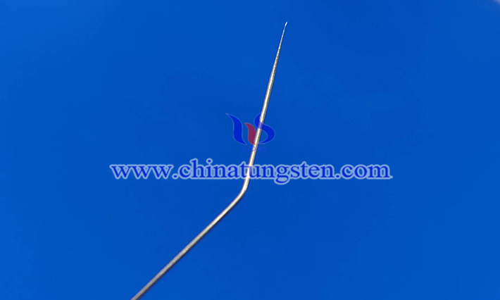
Define the characteristics of the tungsten tips. Consider the size, shape, and sharpness of the tips based on the dimensions and design of the LED components on the wafer.
Consider Flexibility and Compliance:
Evaluate the need for flexibility and compliance in the probe design. LED wafers may have variations in surface height or contour, so probes should be designed to adapt to these variations without causing damage.
Address Contact Force:
Determine the required contact force during testing. LED components can be sensitive, so probes with low-contact-force characteristics may be preferable to avoid damaging the structures.
Fine-Tune for Pitch and Density:
If the LED structures have fine pitches or high-density arrangements, ensure that the probes can make accurate and reliable contacts without causing shorts or damage.
Review Compliance Standards:
Ensure that the customized probes comply with industry standards and requirements for wafer testing. This may include standards related to electrical performance, materials, and safety.
Collaborate with Manufacturers:
Work closely with manufacturers or suppliers experienced in producing customized tungsten probes. Provide them with detailed specifications and collaborate on the design to ensure the probes meet the desired criteria.
Prototype and Test:
Before mass production, create prototypes of the customized probes and conduct testing on sample LED wafers. This step allows for refinement and adjustment of the probe design to ensure optimal performance.
Optimize for Cost and Efficiency:
Consider factors such as cost-effectiveness and manufacturing efficiency during the customization process. Optimize the design to achieve the desired performance while managing costs.
Chinatungsten Online is a professional manufacturer of tungsten and molybdenum for nearly thirty years. We can supply various kinds of tungsten needles as per the drawings. Please free feel to contact us when you got the purchasing plans.


